Showing posts with label semiconductor. Show all posts

Friday, December 20, 2019

Baidu and Samsung release AI chip, designed based on Samsung’s 14nm process and I-Cube package technology

Chinese-language Internet search provider Baidu and Samsung Electronics announced that Baidu’s first cloud-to-edge AI accelerator, Baidu KUNLUN, has completed its development and will be mass-produced early next year.

Baidu KUNLUN chip is built on the company’s advanced XPU, a home-grown neural processor architecture for cloud, edge, and AI, as well as Samsung’s 14-nanometer (nm) process technology with its I-Cube (Interposer-Cube) package solution.


The chip offers 512 gigabytes per second (GBps) memory bandwidth and supplies up to 260 Tera operations per second (TOPS) at 150 watts. In addition, the new chip allows Ernie, a pre-training model for natural language processing, to infer three times faster than the conventional GPU/FPGA-accelerating model.

Leveraging the chip’s limit-pushing computing power and power efficiency, Baidu can support a variety of functions including large-scale AI workloads, such as search ranking, speech recognition, image processing, natural language processing, autonomous driving, and deep learning platforms like PaddlePaddle.


Through the first foundry cooperation between the two companies, Baidu will provide advanced AI platforms for maximizing AI performance, and Samsung will expand its foundry business into high performance computing (HPC) chips that are designed for cloud and edge computing.

As higher performance is required in diverse applications such as AI and HPC, chip integration technology is becoming more and more important. Samsung’s I-Cube technology, which connects a logic chip and high bandwidth memory (HBM) 2 with an interposer, provides higher density/ bandwidth on minimum size by utilizing Samsung’s differentiated solutions.

Compared to previous technology, these solutions maximize product performance with more than 50 percent improved power/signal integrity. It is anticipated that I-Cube technology will mark a new epoch in the heterogeneous computing market. Samsung is also developing more advanced packaging technologies, such as redistribution layers (RDL) interposer and 4x, 8x HBM integrated package.


“We are excited to lead the HPC industry together with Samsung Foundry,” said OuYang Jian, distinguished architect of Baidu. “Baidu KUNLUN is a very challenging project since it requires not only a high level of reliability and performance at the same time, but is also a compilation of the most advanced technologies in the semiconductor industry. Thanks to Samsung’s state of the art process technologies and competent foundry services, we were able to meet and surpass our goal to offer superior AI user experience. ”

“We are excited to start a new foundry service for Baidu using our 14nm process technology,” said Ryan Lee, vice president of Foundry Marketing at Samsung Electronics. “Baidu KUNLUN is an important milestone for Samsung Foundry as we’re expanding our business area beyond mobile to datacenter applications by developing and mass-producing AI chips. Samsung will provide comprehensive foundry solutions from design support to cutting-edge manufacturing technologies, such as 5LPE, 4LPE, as well as 2.5D packaging.”


Sunday, December 8, 2019

Keysight, Marvin Test Solutions come together to speed manufacturing of mmWave semiconductors

Keysight Technologies announced this week that its collaboration with Marvin Test Solutions Inc. (MTS) – a supplier of functional test solutions – has resulted in the development of a fast and accurate 5G semiconductor manufacturing test platform.

The two parties focused on advancing beamformer integrated circuit (IC) test technology to help manufacturers of semiconductors accelerate the production of high performance 5G integrated ICs. Marvin integrated Keysight’s PXIe-based Vector Network Analyzer (VNA) to achieve accurate and fast measurements in its TS-960e-5G mmWave Test System.


The Keysight M980xA PXIe Vector Network Analyzer (VNA) meets the most demanding multiport challenges with a true multiport architecture that offers exceptional performance no matter how many ports you use. Gain deeper insights into devices with the widest available line of measurement applications for PXI VNAs, including spectrum analysis and noise figure measurements.

The M980xA Series offers the performance required for testing passive components, amplifiers, mixers or frequency converters. It provides key PXI VNA specifications such as dynamic range, measurement speed, trace noise and temperature stability. 


Keysight’s recently introduced M980xA Series network analyzers offer the scalability required to test multi-port components, front end modules (FEMs) and base stations that rely on beamforming technology. Mobile operators are deploying beamforming technology to extend cellular coverage and deliver higher data rates, leading to improved mmWave 5G network reliability and efficiency. 

To ensure reliable and efficient 5G mmWave communications, the performance of critical elements that form part of the beamformer IC need to be rigorously tested under linear and nonlinear conditions across the entire workflow from design, validation to manufacturing.


“Our collaboration with Marvin Test Solutions demonstrates that scalable production testing of beamformer solutions can be achieved with Keysight’s PXI VNAs,” said Kailash Narayanan, vice president and general manager of Keysight's wireless test group. “We’re excited to help shape the future of 5G mmWave production testing with our beamformer IC test solutions using integrated component and system-level simulation tools to deliver high precision measurements at mmWave frequency bands.”

Wednesday, October 30, 2019

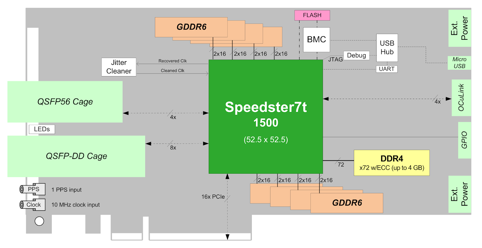
BittWare, Achronix introduce enterprise-class PCIe accelerator product featuring 7nm Speedster7t FPGA

BittWare, a Molex company, has collaborated with Achronix Semiconductor to introduce the S7t-VG6 PCIe accelerator product—a feature-rich PCIe card sporting the new Achronix 7nm Speedster7t FPGA. 

This next generation product offers a range of breakthrough capabilities including low-cost and highly flexible GDDR6 memories that offer HBM-class memory bandwidth, high-performance machine learning processors and a revolutionary 2D network-on-chip for high bandwidth and energy-efficient data movement.


The S7t-VG6 offers a 7nm Achronix FPGA that is optimized for high-speed networking and fast, high-capacity memory access. Featuring a QSFP-DD (double-density) cage, the board supports up to 1x 400GbE or 4x 100GbE using the 56G PAM4-enabled Speedster 7t device. 

An additional QSFP port supports 2x 100GbE, and a 4x OCuLink connector supports NVMe attached storage. Sixteen channels of GDDR6 graphics DRAM handle high-bandwidth memory requirements, providing up to 512GB/s.


The BittWare VectorPath accelerator card is designed for high-performance and high-bandwidth data applications and features 1x400GbE and 2x100GbE interfaces; 8 banks of GDDR6 memory with 4 Tbps aggregate bandwidth; 20 Tbps 2D Network-on-Chip (NoC); 1 bank of DDR4 running at 2666MHz with ECC; PCIe compliance and certification; and 692K 6-input LUTs.


This enterprise-class product leverages BittWare’s extensive experience designing, qualifying, deploying and supporting accelerator cards. Its features include choice of thermal cooling options: passive, active or liquid; comprehensive Board Management Controller (BMC); support for Linux and Windows operating systems; developer toolkit: API, PCIe drivers, application example designs and diagnostic self-test; and option to purchase the S7t pre-integrated as a DELL or HPE server from BittWare TeraBox range.

The initial S7t-VG6 shipments are scheduled to begin by the second quarter of next year. 

Friday, October 25, 2019

Renesas expands access of IP solutions including 7nm process TCAM, advanced standard Ethernet TSN IPs

Renesas Electronics announced expanded access to its highly sought portfolio of intellectual property (IP) licenses that allow designers to meet a broad range of customer requirements in a rapidly changing industry. Starting today, customers will have access to IPs such as advanced 7nm (nanometer) SRAM and TCAM, and standard Ethernet time-sensitive networking (TSN) IP. 

Furthermore, Renesas is working on providing a system IP which includes PIM (processing in memory), which attracted attention as an AI accelerator, presented in a conference paper in June 2019. With these IPs, customers can jump start their advanced semiconductor device development projects, such as the development of next-generation artificial intelligence (AI) chips or ASICs for 5G networks.


The Renesas accelerator is based on the processing-in-memory (PIM) architecture, an increasingly popular approach for AI technology, in which multiply-and-accumulate operations are performed in the memory circuit as data is read out from that memory.

Customers developing custom chips or using FPGA devices for early development can leverage Renesas IP in their subsystem design or speed up software development, respectively, allowing them to focus resources on their speciality areas, speed up the development process, and bring highly competitive products to market. 


Customers who prefer to use existing software assets can take advantage of Renesas IP assets to achieve more efficient system development by reducing the resources required to develop, verify, and evaluate software and boards.

To support customers’ semiconductor development efforts, Renesas has also established a network of partner companies ready to support users' unique needs. This network includes design houses that perform contract semiconductor design and technology partners who will provide an array of software and middleware tools. 


This network will accelerate users' technology innovations and product development efforts by lowering the barriers to entry for semiconductor device and FPGA development. Renesas can also introduce experienced users to model-based design development environments that fully utilize leading-edge IP.

In September 2018, Renesas opened its extensive IP license portfolio, offering access to more than 40 licenses, including CPU cores, timer IP for motor applications, USB cores, and SRAM. In 2019, Renesas received over 100 enquiries and have started supplying IPs to many users. Renesas aims to exceed IP sales annual market growth rate of 10 percent, and will expand the provision of IP and support system while creating new, and expanding old, IP markets.

Masimo secures FDA clearance for neonatal RD SET Pulse Oximetry sensors with improved accuracy specifications

Masimo announced that RD SET sensors with Masimo Measure-through Motion and Low Perfusion SET pulse oximetry have received FDA clearance ...